Every now and the I get asked, how I make my printed circuit boards (PCB). Here I give a tutorial on how I achieve verry good results.
For the impatient of you, here is a short overview:
I am using a positive photo-lithographic process to transfer the artwork to a photosensitized, copper cladded PCB laminate. Positive means, that during the development step the protective coating on the copper is removed in those places that were previously exposed to UV light. So the artwork has to block UV light where you want the traces on the board.
The stuff I use:
- Bungard PCB laminate, thickness 0.5mm - 1.5mm with a copper cladding of 35µm - 70µm, positive type photo resistive
- Artwork printing with a HP P2055d on Avery/Zweckfrom #3491
- Toner darkener: Conrad #528017
- Exposing on gie-tec "UV-Exposure Box 2" for 160sec
- Development with NaOH 10g/l for 60 sec
- Etching using Na(SO4)2 in 7-15 min
- Acid tinning using Bungards "SurTin" 3 min
- Lamination of solder stop "Dynamask" with a normal bureau laminator
- Exposure of the solder stop for 45 sec
- Development of the solder stop with NaCO3 10g/l in 2 min
- UV curing the solder stop for 30min
- Thermal curing at 140°C for 30 min
- Drilling using tungstan carbid drills
- Interlayer connection with silvered copper wire
On the following pages I will picture every step and detail the important parts.
1. CHEMICAL SAFETYThese processes involves the use of different chemicals (NaOH, NaS2O8, NaCO3, acetone), some of which may cause severe eye damage, irritation of the skin or holes in clothings. Always handle chemical with the appropriate respect and always wear adequate protection: Safety googles and latex gloves are mandatory, a lab coat is recommended. After use dispose the chemical solutions of properly, especially the etchant will contain a lot of copper ions which are extremly toxic and under no circumstances may be flushed down the drain. Contact your local collecting point for toxic waste if unsure!
2. GENERATING THE ARTWORKBefore you can build your PCB you will have to create the artwork, that is decide where the individual tracks will be placed on the final board, and where the individual electrical components (connectors, passive components, ICs, etc) are located. This step means you have to create a schematic diagram of the circiut, and create a board layout off this schematic.
There are numerous CAD programs to assist you in this process, currently I am using an old version of EAGLE (4.16) of Cadsoft. Once you have designed your artwork, you will have to print it to a transparency in a way, that the transparency becomes intransparent where you want a copper track on the board. Because of two reasons I am using a laser printer for this task: Laser printers offer a good coverage and there is no drying ink in case I do not use the printer for a while. However you have to be a bit careful: The toner usually does not stick to those standart glossy transparanys very well, so this will result in a very poor master. For this reason I am using the Avery/Zweckfrom #3491 films that are intended for print master production. They have a matte surface, and the toner adheres reliable to them.
When printing your masters, you want all the top layer artwork to be printed mirrored, since this will lead to the toner laying directly on the photo sensitive board resulting in sharp contrasts when exposed. Since I am going to make a double sided board with solder stop I have four master films printed: Top and bottom copper, and top and bottom solder mask.
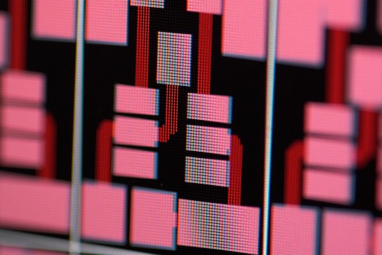
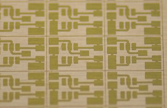
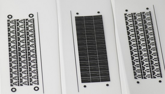 In the above picture you can see three of the four films I use in this tutorial. (Please note, that the solder stop film is a negative type, that is it is beeing removed in the process in those places which do not get exposed to UV light.) Although using those special films you may find that the print is not as covering as you want it to be. Since a non covering film will lead to small holes in traces and pads on the board you want to darken the toner somehow. One option is to print the layout twice and stack the two films, an other one is to use toner darkener (sounds magic - doesn't it?):
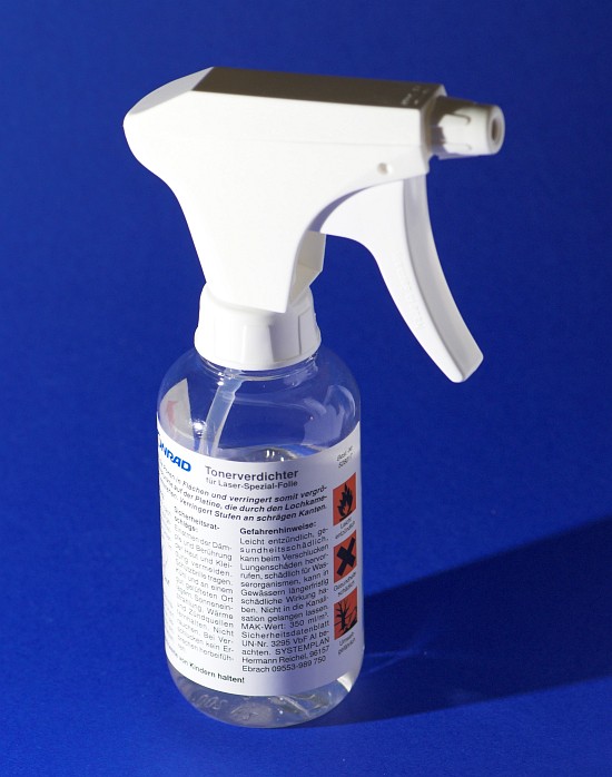 Place the film on a level base and spray the toner darkener evenly on the film. The darkener is basically a solvent that dissolves the toner particles and when dried leaves a dense black area where the toner was. It is quite interesting, but you do not get any bleeding of the toner. Place your cursor on the following picture to get an impression how well this works. It is astounding!
Now you have to align the film for the top and bottom side of the PCB: On a well lit working place, align both films to each other and secure them using adhesive tape.
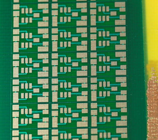
3. EXPOSURE AND DEVELOPMENTNext, prepare the PCB. The base material I use is a double sided photo sensitized copper cladded board from Bungard. It is a standard FR4 material, which means it is made of woven glass reinforced epoxy. The material from Bungard has the advantage of a consistent quality and a high resolution. This results in sharp traces on the board.
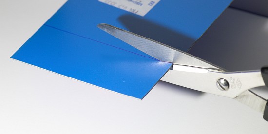
If you have, the easieset way to cut the PCB is using a metal shear like used to cut aluminum plates, but you can use a saw, too. In case you use a saw, be sure to not remove the blue protective masking by accident, since this will expose and/or scratch the damageable photo sensitive coating. For the thin (0.5mm) material I am using normal scissors. This works fast, without any saw dust and does not harm the coating as well.
 Carefully peel off the protective layers of the board and place the board betwen the two tacked films. Secure the board so that it can not move using adhesive film. (Please note, that with the protective Layer removed the PCB is sensitive especially to blue and UV light. Do only handle it in dim light.)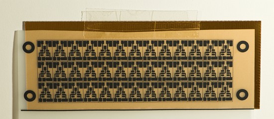 Now the board is exposed to UV light. After experimenting a lot with UV LEDs I found it much easier and more reliable to use a commercial UV exposure device from gie-tec that contains 4 fluorescent tubes each having 15W electrical power consumption.The actual exposure time depends on the your current setup: Sensitivity of the PCB, transmissibility of the film, luminous intensity of the light source, concentration and temperature of the developer (see later). For my setup, a exposure time of 160 seconds each side yields the best results, but your times may vary. You may perform an exposure series to find the correct settings.After the exposure of both sides remove the master film and you will notice that the coating has brightened were it was lit by the UV light. To develop the board use a sodium hydroxide solution of 10g/l. Usually I only prepare 200ml of this solution as this is enough for about 5 double sided boards of 16cm x 10cm. Weight 2.0g of the NaOH flakes in a 300ml beaker, and add 200ml of cold tap water. Continue to stir the solution until all the NaOH is dissolved. Be sure to wear safety googles since NaOH causes severe eye damages even in this low concentration!
Pour the developer in a flat bowl and dip the PCB completely in the solution - I did the partial immersion only for the picturs. Within the first 3 seconds you will see the exposed coating dissolving in red clouds. Slowly move the board in the soulution to develop every part of the PCB and to achive a uniform result. Measure the time until the board looks completely developed, and allow it to stay in the solution for the same ammount of time thereafter. At this point you should not see any more of the coting being dissolved (no red borders on the traces).
Once completed, rinse the board with clear, cold water. Do not swipe across the board since the coating is easily damaged. Also do not dry the board, as this is not necessary an may scratch the board.
 4. ETCHING AND TINNINGFor etching of the PCBs I am using a cuvette filled with a aqueous solution of 600g sodium persulfate Na(SO4)2 per 1.5l of water. The persulfate has to be heated to 45°C in order to eat away the copper, so there is a small heater in the cuvette. To keep the solution moving I have a bit of air bubbeling from the bottom of the cuvette. All the stuff (heater, air pump) can be found as accessory for aquaria.
The process takes some time. Depending on the temperature and the wear level of the solution the times vary between 7 min and 15 min. (Note: There are faster etchants, like hot ferric trichloride or a mixture of hydrochloric acid and hydrogen peroxide. But they all leak small ammounts of chlorine or hydrochloric acid which will slowly corrode all iron tools in your laboratory. Unless you do have a well vetilated storage room, I strongly recommend to not use those etchants at home.)
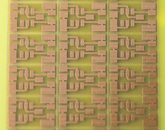
Carefully observe the progress of the etching process. Once all copper that is not protected by the coating is removed, take the PCB out of the cuvette and rinse it.
Now you need to remove the coating on top of the traces: You can either use acetone which dissolves the varnish, but I prefer to expose the board a second time, but this time without any film. After this exposure just develop it again in the same solution as before. This way you end up with a perfectly clean copper surface without any schlieren.
 A very clean surface is extremly important for the following acid-tinning. For this I use a comercially available chemical kit (Sur-Tin from Bungard) consisting mainly of sulphuric acid, thiourea, tin(II) chloride and additives. Follow the instructions when obtaining this stuff to prepare the tinning bath. After the second development very thoroughly rinse the board with fresh water and without drying dip it directly in the tinning solution. Keep it in there for about 3 min and move the PCB every now and then. Take out the board and rinse it again.
At this point the board is ready to use, however you may want to apply a solder stop mask and/or drill the board.
5. SOLDER STOP
The solder stop is a clear, green, tin repellant coating that is applied on top of the copper traces. This is done to prevent solder bridges (especially on SMD components) and to reduce leakage currents due to moisture on the FR4 surface. The solder stop film consists of three layers: A clear 25µm protective polyester film on top, an opaque 25µm polyolefine coating on the bottom and the 75µm thick translucent green photopolymer resist. As far as I know, the photopolymer consists mainly of prepolymers and the photoactive curing agent.
Before lamination be sure you have a clean PCB that is very dry. Usually I feed the PCB a few times through the hot laminator to remove any moisture, but you can bake it in an oven at 100°C just as well. If there is even a tiny little bit of moisture in the PCB you will get gas bubbles under the solder stop. Next, remove the opaque protective film of the solder stop. It is important to remove this exact coating becuse the polyolefine would melt during the lamination process. Attach a piece of adhesive on top and bottom of a corner of the solder stop film, and carefully pull both strips apart. You may need several attempts for this, but do not desperate: It will work. You may also try different corners.
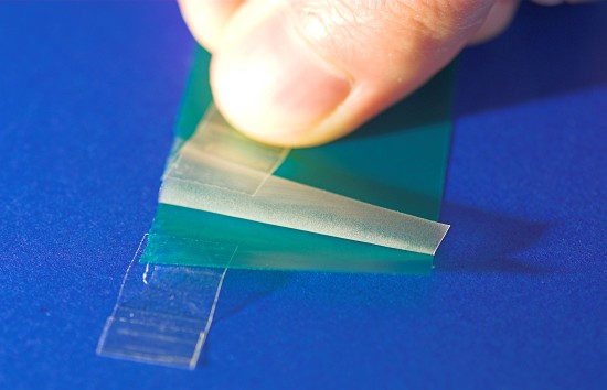 Only remove the opaque film about 1-2cm. You will find that the surface of the green coat is very sticky and easily adheres to all available surfaces. Once placed on the board, you will not be able to remove it again. Carefully align the stripe of solder stop to the PCB and with a gentle press attach the 1cm wide expose stripe to the board. To avoid any air being trapped under the film you want the laminator to press the film on to the board. So avoid any eccessive contact between the solder stop film and the board.
Now there comes a tricky part: Feed the board with the edge where the solder stop adheres to it in the pre-heated laminaor while carefully pulling back the polyolefine layer between the solder stop and the board.
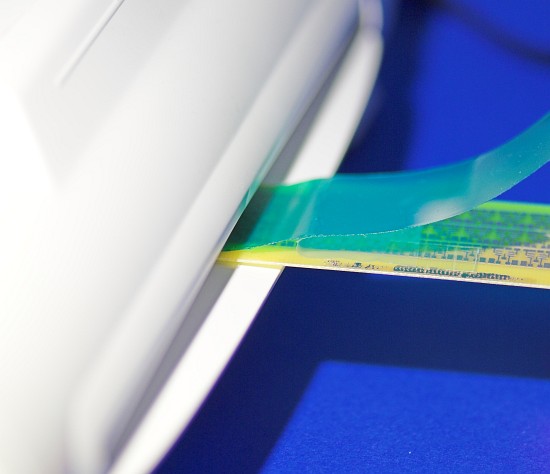 You should end up with a perfectly even green coating not containing any bubbles. Allow the PCB to cool down, and then repeate the step for the back side.
Now align the top and bottom solder stop master to the underlying copper traces and secure it with some adhesive
On my exposure box I expose each side for 40 seconds. When exposed to UV light (350nm - 400nm) the polymers crosslink and the resist hardens so that it will not be removed during the development step.
After the exposure let the film cure for about 15 min - 30 min. If you are in a hurry and do not stick to these times you may encounter undercutting. Remove the top and bottom protection layers afterwards.
The developing of the solder mask is done in a solution of 10g sodium carbonate (Na2CO3) per 1l water. As an alternative you can also use an equally concentrated solution of sodium silicate (Na2SiO3) - the NaOH from developing the etch resist does not work: It will dissolve the solder stop completely. Heat up the developer to about 40°C and immerse the board in the solution. After a few seconds the non hardened parts will form a greyish cloud above the pads, I use a soft acrylic brush to remove it. Gently swipe across the surface until the PCB is completly developed. Using tweezers, turn over the PCB and repeat for the other side as well.
Once both sides are developed, rinse the board thoroughly and dry it. The board looks finished now, but the solder stop still has to be cured: Expose each side for 30 minutes to the UV light and bake the board in an oven at 140°C for 30 minutes. I am using a small non-modded pizza oven for this. Do not use any oven you want to prepare food afterwards with for this baking: The fumes are harmfull. This process assures a completely cured solder stop mask that survives soldering and protects your board.
6. POST PROCESSINGThere is not much left to say: Cut the PCB to the desired size, drill if neccessary (this section is coming soon) and make interlayer connections where necessary. |


